- +64 9 269 6916
- +64 9 269 6926
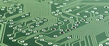
Learn about printed circuit board and stencil technology and empower your business!
PCB Technology
Glossary and Abbreviations - PCB Glossary
Click on an alphabet below to directly jump to the chosen alphabet section...
ABCDEFGHIJKLMNOPQRSTUVWXYZAlphabet C
- CAD – (Computer Aided Design)A system where engineers create a design and see the proposed product in front of them on a graphics screen or in the form of a computer printout or plot. In electronics, the result would be a printed circuit layout.
- CAM – (Computer Aided Manufacturing)The interactive use of computer systems, programs, and procedures in various phases of a manufacturing process wherein, the decision making activity rests with the human operator and a computer provides the data manipulation functions.
- CAM FilesThe data files used directly in the manufacture of printed wiring. The file types are: (1) Gerber files, which control a photoplotter. (2) NC Drill file, which controls an NC Drill machine. (3) Fabrication drawings in Gerber, HPGL or any other electronic format. Hard copy prints may be available also. CAM files represent the final product of PCB design. These files are given to the board house which further refines and manipulates CAM in their processes, for example in step and repeat panelization.
- ChamferA broken corner to eliminate an otherwise sharp edge.
- CardAnother name for a printed circuit board.
- CapacitanceThe property of a system of conductors and dielectrics that allows the storage of electricity when a potential difference exists between the conductors.
- CatalystA chemical that is used to initiate the reaction or increase the speed of the reaction between a resin and a curing agent.
- Ceramic Ball Grid Array (CBGA)A ball grid array package with a ceramic substrate.
- CEM1orCEM3PCB board materials, standard epoxy resin with woven glass reinforcement over a paper core, differing only in the type of paper used. They are less expensive than Fr4.
- Center to Center SpacingThe nominal distance between the centers of adjacent features on any single layer of a printed board, e.g.; gold fingers and surface mounts.
- Check PlotsPen plots, or plotted film, that are suitable for checking and for design approval by customers.
- Chip on Board (COB)A configuration in which a chip is directly attached to a printed circuit board or substrate by solder or conductive adhesives.
- Check plotsPen plots that are suitable for checking only. Pads are represented as circles and thick traces as rectangular outlines instead of filled in artwork. This technique is used to enhance transparency of multiple layers.
- ChipAn integrated circuit manufactured on a semiconductor substrate and then cut or etched away from the silicon wafer. (Also called a die.) A chip is not ready for use until packaged and provided with external connections. Commonly used to mean a packaged semiconductor device.
- Chip scale packageA chip package in which the total package size is no more than 20% greater than the size of the die within. Eg: Micro BGA.
- CircuitA number of electrical elements and devices that have been interconnected to perform a desired electrical function.
- Circuit BoardA shortened version of PCB.
- CIM (Computer Integrated Manufacturing)Used by an assembly house, this software inputs assembly data from a PCB CAM/CAD package, such as Gerber and BOM, as input and, using a predefined factory modeling system, outputs routing of components to machine programming points and assembly and inspection documentation. In higher end systems, CIM can integrate multiple factories with customers and suppliers.
- Circuitry LayerA layer of a printed board containing conductors, including ground and voltage planes.
- CladA copper object on a printed circuit board. Specifying certain text items for a board to be "in clad," means that the text should be made of copper, not silkscreen
- ClearancesA clearance (or isolation) is a term we use to describe the space from power / ground layer copper to through hole. To prevent shorting, ground and power layer clearances need to be .025” larger than the finish hole size for the inner layers. This allows for registration, drilling, and plating tolerances.
- Clearance HoleA hole in the conductive pattern that is larger than, and coaxial with a hole in the base material of a printed board.
- CNC (Computer Numerical Control)A system that utilizes a computer and software as the primary numerical control technique.
- ComponentAny of the basic parts used in building electronic equipment, such as a resister, capacitor, DIP or connector, etc.
- Component HoleA hole that is used for the attachment and/or electrical connection of component terminations, including pins and wires, to a printed board.
- ComponentSideIn order to prevent building a board inside out, we must be able to identify the correct orientation of your design. Component, layer 1, or 'top' layer should read in facing up. All other layers should line up as though looking through the board from the topside.
- Conductive PatternThe configuration pattern or design of the conductive material on a base material. (This includes conductors, lands, vias, heat sinks and passive components when those are integral parts of the printed board manufacturing process.
- Conductor SpacingThe observable distance between adjacent edges (not center to center spacing) of isolated patterns in a conductor layer.
- ContinuityAn uninterrupted path for the flow of electrical current in a circuit.
- Conformal CoatingAn insulating & protective coating that conforms to the configuration of the object coated and is applied on the completed board assembly.
- ConnectionOne leg of a net.
- ConnectivityThe intelligence inherent in PCB CAD software which maintains the correct connections between pins of components as defined by the schematic.
- ConnectorA plug or receptacle, which can be easily joined to or be separated from its mate. Multiple contact connectors join two or more conductors with others in one mechanical assembly.
- Connector AreaThe portion of the circuit board that is used for providing electrical connections.
- Controlled ImpedanceThe matching of substrate material properties with trace dimensions and locations in an effort to create specific electric impedance for a signal moving along a trace. Conventional PCB: A rigid PCB with thickness 0.062” with wire leaded components, mounted only on one side of PCB, with all lead through hole soldered and clipped. Conventional circuitry is easier to debug and repair the surface mount.
- Core ThicknessThe thickness of the laminate base without copper
- CoatingA thin layer of material, conductive, magnetic or dielectric, deposited on a substance surface.
- Coefficient of Thermal Expansion (CTE)The ratio of dimensional change of an object to the original dimension when temperature changes, expressed in %/ºC or ppm/ºC.
- Contact Angle (Wetting Angle)The angle between the contact surfaces of two objects when bonding. The contact angle is determined by the physical and chemical properties of these two materials.
- Copper Foil (Base Copper Weight)Coated copper layer on the board. It can either be characterized by weight or thickness of the coated copper layer. For instance, 0.5, 1 and 2 ounces per square foot are equivalent to 18, 35 and 70 um:thick copper layers.
- CopperFoilFinished copper weight = 1oz.
- Control CodeA non-printing character which is input or output to cause some special action rather than to appear as a part of data.
- Core ThicknessThe thickness of the laminate base without copper.
- Corrosive FluxA flux that contains corrosive chemicals such as halides, amines, inorganic or organic acids that can cause oxidation of copper or tin conductors.
- CrosshatchingThe breaking up of large conductive area by the use of a pattern of voids in the conductive material.
- CuringThe irreversible process of polymerizing a thermosetting epoxy in a temperature time profile.
- Curing TimeThe time needed to complete curing of an epoxy at a certain temperature.
- CutlinesA cut line is what our system uses to program the router specifications. It represents the outer dimensions of your board. This is required for the board to finish as the size you want it.
PCB Design Tips
When designing a PCB, try to limit the amount of draws you use. Draws use a lot of memory and slow the programming time. Use a flash for pads instead.
More tips...
Contract Assembly
We are one-stop solution provider for all your contract assembly requirements. We have the capability and resources to provide PCB assemblies, as well as cable and harness assemblies.

What our customers say?
QualiEco Circuits Limited is an excellent supplier to us! We appreciate the quality of service and support that we receive from QualiEco Circuits. They always deliver what is promised
For printed circuit boards (PCBs) or PCB assembly you can count on. Talk to the friendly and experienced team at QualiEco Circuits, New Zealand.